Radiant Advanced Devices Sdn Bhd
24, Jalan Imigresen,
10400 Georgetown,
Pulau Pinang, Malaysia.
+60 4 210 1390
+60 4 210 1391
OmegaPrep
| Previous | 1 / 4 | Next |
We don’t break die
The OmegaPrep was designed to perform in package die thinning and polishing in addition to a number of machining functions for sample preparation. The die thinned and polished by the OmegaPrep are compatible with all backside procedures such as IR emission microscopy and FIB edit. OmegaPrep can also perform mechanical decapsulation, removal of heat spreaders and heat sinks, and can easily remove plastic packaging and die attach pad to expose the die. Additional capabilities have been included that provide processes for die de-layering &/or de-processing; substrate or PCB delayering; fixture machining; selected area thinning to 1µm remaining silicon, and more.
OmegaPrep is a specially designed, CNC machining system controlled by a graphic user interface that allows for the operator to select the desired functions and enter the key device measurements and process parameters. There is no need to know anything about machining or “G Code” to operate the OmegaPrep. There are no knobs to adjust, or cranks to turn. ‘Speeds and Feeds’ are preset for each process to optimize processing results.
Automatic tool touch-down detection, video alignment and special profiling functions make set-device set up simple and easy. The surface profiling function eliminates the need for die leveling and maintains a constant resulting thickness for both die thinning and consistent layer removal during delayering processes.
Die as large as 44mm (square) and delayering and machining areas up to 55mm square can be accommodated. Packages up to 150mm long x 125mm wide can be mounted on the standard fixtures supplied with the system. Custom fixtures can be supplied for even larger devices.
- Die thinning and polishing
- Local area thinning to 1µm remaining silicon
- Optional silicon measurement systems for best thickness control
- Encapsulant and die attach removal
- Heat sink removal
- Substrate and PCB delayering
- Substrate removal
- Stacked die removal
- C4 ball exposure
- Die de-layering or de-processing
- Automatic leveling and surface profile measurement
- Optional, in situ, silicon thickness measurement
- Simple sample mounting and alignment
- Process recipes can be saved for later use
At the beginning of each process, the OmegaPrep will measure the surface profile of the sample. This is done by contacting the surface at discrete points and recording the surface height at each measured point. The touch tool used has a spherical tip to eliminate surface damage from such contacts. The measured profile points are used to generate a ‘wire frame model’ representation of the surface that is subsequently used to generate the three dimensional path of the tool tip during process. The measurement of the surface profile completely eliminates the need for any sample leveling adjustments. The number of measured points and their positions are selected by the OmegaPrep on the basis of the sample size and the process to be run. For very small samples, only four points are measured. The four points are used to define the average plane of the surface and is all that is required as the variation in surface profile from a plane is limited by the mechanical properties of the sample.
Between the process steps during die thinning, the sample holder and sample are removed for cleaning. Often, due to possible particulates trapped between the sample holder and the stage, the sample profile may be rotated slightly from the initial profile measurements. This is corrected for by measuring a small number of points on the surface and mathematically rotating the stored profile to match. Some processes allow for the operator to input silicon thickness measurements. The optional thickness measurement systems can be used to measure the remaining silicon thickness. The thickness profile, either entered by the operator, or measured by the OmegaPrep, will be used to correct the mechanical surface profile to maintain a constant silicon thickness over the area being processed.
Once the device and process parameters, die size, die position, die attach pad size, amount of removal, etc., have been programmed, they can be saved as a process recipe. The recipe can be recalled for reference, or duplication of the processing for a different sample. Up to 96 recipes can be stored in the OmegaPrep, each with a unique, operator generated name.
During the processing of a sample, all parameters and operator actions can be saved for future printing or review. This leaves a complete history of each sample processed.
AI ACCELERATOR CHIPS AND THE FUTURE
The opportunity for AI accelerator chips is much-hyped, but how big is the market, and which companies are actually selling chips today. Two reports from ABI Research detail the state of play for today’s AI chipset market.
Whatever the future holds, Failure Analysis of these devices and their associated interconnects will become ever more important in future technological advances. Thus equipment such as the RKD Systems OmegaPrep and the UltraPrep III will be essential tools in the development of AI’s and associated chip sets for both isolated chips as well as the ability to examine chip on flex circuitry for the failure analysis of these advanced products.
We can now offer todays tools for today’s packages, rather than re-vamped, old technology kludged together in an attempt to meet the requirements for advanced chip sets and their associated circuitry.
AI IN THE CLOUD
The AI chipset market is expected to grow from approx.US$4.2 billion (2019) to US$10 billion (2024). Nvidia and Intel, the present leaders, are being challenged by companies including Qualcomm, Cambricon Technologies, Graphcore, Habana Labs. Nvidia is still the leader in this market, as a result of its well-established developer ecosystem.
As AI models, toolkits and libraries are updated Nvidia serves as a good option, given its capability as a general-purpose AI chipset. Whilst such advantages may slowly change as this market matures, Nvidia will remain be in a strong position for at least the foreseeable future.
Today the cloud market for AI chipsets can be divided into 3 segments. The public cloud, as hosted by cloud service providers e.g. Microsoft, Google, Alibaba, Baidu, Tencent and others. Enterprise Data Centers, which are effectively private clouds, and what had been termed “hybrid clouds,” meaning options that combine public and private clouds (e.g. VMware, NetApp, Dell).
An an additional emerging segment called – Telco Clouds has also been identified that refers to cloud infrastructure, as deployed by telecom companies for their core own network cores and corporate computing workloads.
We have already seen network infrastructure vendors like Huawei (and to a lesser extent Nokia) adopting ASICs optimized for telco network functions.

Annual revenue for AI Chip Set Sales, 2017-2024 (Source: ABI Research)

Annual revenue for AI Chip Set Sales, 2017-2024 (Source: ABI Research)
ASIC sales are predicted to show strong growth in this sector from 2020 onwards. The current trend for moving AI inference to edge devices will mean less reliance on the cloud from devices such as smartphones, autonomous vehicles and robots. But this does not mean that the inference workload, which some cloud service providers deem to be larger than training workload, is going to diminish, according to Lian Jye Su of ABI Research, Singapore.
Further Su commented that “Some AI will never move to the edge, such as chatbots and conversational AI, fraud monitoring and cybersecurity systems. “These systems will evolve from rule-based to deep learning-based AI systems, which actually increases the inference workload. This increase will be more than sufficient to replace those inference workloads that move to the edge.”
Google’s TPU (tensor processing unit), which can address both training and inference in the cloud, is seen as a strong challenger for CPU and GPU technologies. As this report noted, Google’s success with the TPU has provided a blueprint for other cloud service providers (CSPs) to develop their own AI accelerator ASICs. Huawei, AWS, Baidu have already done this.
If the cloud service providers are all working on their own chipsets, does that leave a market for any other chipset suppliers in that sector?
“You are certainly right that this path has been very challenging for newcomers, as CSPs start to work on their own chipsets,” Su said. “ABI Research forecast that 15% – 18% of the market will fall under the CSPs by 2024. The opportunity lies more in the private data center space. Banking institutions, medical organizations, R&D labs and academia will still need to run AI and they will be considering chipsets that are more optimized for AI workloads, which gives newcomers like Cerebras, Graphcore, Habana Labs & Wave Computing some advantages.”
Other players that will benefit from these trends are IP core licensing vendors, like ARM, Cadence and VeriSilicon, where they will be responsible for chipset design for even more chipset-developing enterprises than before.
AI at the Edge [for a definition of Edge Computing please see https://en.wikipedia.org/wiki/Edge_computing]
ABI Research have also reported on the technology of Edge AI Chipsets,
“Edge AI Chipsets: Technology Outlook and Use Cases,” puts the Edge AI inference chipset market at US$1.9 billion in 2018. Which applications are doing training at the edge today? Su explained that this figure includes gateways (device hubs) and on-premise servers (in private clouds, but geographically located where the AI data is generated). Chipsets designed for training tasks on on-premise servers include Nvidia’s DGX, Huawei’s gateways and servers which feature their Ascend 910 chipset, and system-level products targeted at on-premise data centers from companies such as Cerebras Systems, Graphcore and Habana Labs. Training at the edge market will remain small, as the cloud is still the preferred location for AI training.

An in-depth look at Google’s first Tensor Processing Unit (TPU)
There’s a common thread that connects Google services such as Search, Street View, Photos and Translate: they all use Google’s Tensor Processing Unit, or TPU, to accelerate their neural network computations behind the scenes.
We announced the TPU last year and recently followed up with a detailed study of its performance and architecture. The TPU delivered 15–30X higher performance and 30– 80X higher performance-per-watt than contemporary CPUs or GPUs. These advantages help many services run state-of-the-art neural networks at scale and at an affordable cost. In this post, we’ll take an in-depth look at the technology inside the Google TPU and discuss how it delivers such outstanding performance.
The road to TPUs
Norm Jouppi, the tech lead for the TPU project (also one of the principal architects of the MIPS processor) described the sprint this way:
- “We did a very fast chip design. It was really quite remarkable. We started shipping the Nrst silicon with no bug Nxes or mask changes. Considering we were hiring the team as we were building the chip, then hiring RTL (circuitry design) people and rushing to hire design veriNcation people, it was hectic. ”
The TPU ASIC is built on a 28nm process, runs at 700MHz and consumes 40W when running. Because we needed to deploy the TPU to Google’s existing servers as fast as possible, we chose to package the processor as an external accelerator card that Nts into an SATA hard disk slot for drop-in installation. The TPU is connected to its host via a PCIe Gen3 x16 bus that provides 12.5GB/s of effective bandwidth.

Prediction with neural networks
For example, if you have three inputs and two neurons with a fully connected single-layer neural network, you have to execute six multiplications between the weights and inputs and add up the multiplications in two groups of three. This sequence of multiplications and additions can be written as a matrix multiplication. The outputs of this matrix multiplication are then processed further by an activation function. Even when working with much more complex neural network model architectures, multiplying matrices is often the most computationally intensive part of running a trained model.

Prediction with neural networks
Let’s look at calculations involved in running a simple neural network.
This example on the TensorFlow Playground trains a neural network to classify a data point as blue or orange based on a training dataset. The process of running a trained neural network to classify data with labels or estimate some missing or future values is called inference. For inference, each neuron in a neural network does the following calculations:
- Multiply the input data (x) with weights (w) to represent the signal strength
- Add the results to aggregate the neuron’s state into a single value
- Apply an activation function (f) (such as ReLU, Sigmoid, tanh or others) to modulate the artiNcial neuron’s activity.
In July 2016, a survey of six representative neural network applications across Google’s production services and summed up the total number of weights in each neural network architecture. You can see the results in the table below.
| Type of network | # of network layers | # of weights | % of deployed |
| MLP0 | 5 | 20M | 61% |
| MLP1 | 4 | 5M | |
| LSTM0 | 58 | 52M | 29% |
| LSTM1 | 56 | 34M | |
| CNN0 | 16 | 8M | 5% |
| CNN1 | 89 | 100M |
(MLP: Multi Layer Perceptron, LSTM: Long Short-Term Memory, CNN: Convolutional Neural Network)
As you can see in the table, The number of weights in each neural network varies from 5 million to 100 million. Every single prediction requires many steps of multiplying processed input data by a weight matrix and applying an activation function.
In total, this is a massive amount of computation. As a first optimization, rather than executing all of these mathematical operations with ordinary 32-bit or 16-bit floating point operations on CPUs or GPUs, we apply a technique called quantization that allows us to work with integer operations instead. This enables us to reduce the total amount of memory and computing resources required to make useful predictions with our neural network models.

Quantization in neural networks
Neural network predictions often don’t require the precision of floating point calculations with 32-bit or even 16-bit numbers. With some effort, you may be able to use 8-bit integers to calculate a neural network prediction and still maintain the appropriate level of accuracy.
Quantization is an optimization technique that uses an 8-bit integer to approximate an arbitrary value between a preset minimum and a maximum value.
Quantization is a powerful tool for reducing the cost of neural network predictions, and the corresponding reductions in memory usage are important as well, especially for mobile and embedded deployments. For example, when you apply quantization to Inception, the popular image recognition model, it gets compressed from 91MB to 23MB, about one-fourth the original size.
Being able to use integer rather than ooating point operations greatly reduces the hardware footprint and energy consumption of our TPU. A TPU contains 65,536 8-bit integer multipliers. The popular GPUs used widely on the cloud environment contains a few thousands of 32-bit ooating-point multipliers. As long as you can meet the accuracy requirements of your application with 8bits, that can be up to 25X or more multipliers.

RISC, CISC and the TPU instruction set

RISC, CISC and the TPU instruction set
Programmability is another important design goal for the TPU. The TPU is not designed to run just one type of neural network model. Rather, it’s designed to be oexible enough to accelerate the computations needed to run many different kinds of neural network models.
Most modern CPUs are heavily inouenced by the Reduced Instruction Set Computer (RISC) design style. With RISC, the focus is to deNne simple instructions (e.g., load, store, add and multiply) that are commonly used by the majority of applications and then to execute those instructions as fast as possible. The Complex Instruction Set Computer (CISC) style as the basis of the TPU instruction set instead. A CISC design focuses on implementing high-level instructions that run more complex tasks (such as calculating multiply-and-add many times) with each instruction. Let’s take a look at the block diagram of the TPU.
The TPU includes the following computational resources:
- Matrix Multiplier Unit (MXU): 65,536 8-bit multiply-and-add units for matrix operations
- Unified Buffer (UB): 24MB of SRAM that work as registers
- Activation Unit (AU): Hardwired activation functions
To control how the MXU, UB and AU proceed with operations, we defined a dozen high-level instructions specifically designed for neural network inference. Five of these operations are highlighted below.
| TPU Instruction | Function |
| Read Host Memory | Read data from memory |
| Read Weights | Read weights from memory |
| MatrixMultiply/Convolve | Multiply or convole with the data and weights, accumulate the results |
| Activate | Apply activation functions |
| Write Host Memory | Write result to memory |
This instruction set focuses on the major mathematical operations required for neural network inference that we mentioned earlier: execute a matrix multiply between input data and weights and apply an activation function.
In short, the TPU design encapsulates the essence of neural network calculation, and can be programmed for a wide variety of neural network models. To program it, we created a compiler and software stack that translates API calls from TensorFlow graphs into TPU instructions.

Parallel Processing on the Matrix Multiplier Unit

Parallel Processing on the Matrix Multiplier Unit
Typical RISC processors provide instructions for simple calculations such as multiplying or adding numbers. These are so-called scalar processors, as they process a single operation (= scalar operation) with each instruction.
Even though CPUs run at clock speeds in the gigahertz range, it can still take a long time to execute large matrix operations via a sequence of scalar operations. One effective and well-known way to improve the performance of such large matrix operations is through vector processing, where the same operation is performed concurrently across a large number of data elements at the same time. CPUs incorporate instruction set extensions such as SSE and AVX that express such vector operations. The streaming multiprocessors (SMs) of GPUs are effectively vector processors, with many such SMs on a single GPU die. Machines with vector processing support can process hundreds to thousands of operations in a single clock cycle.
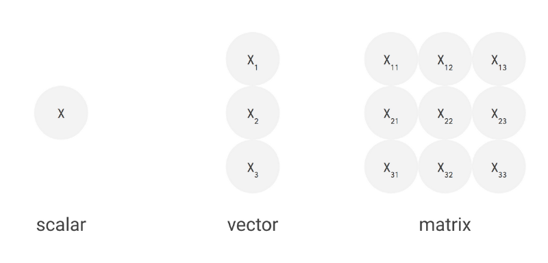
In the case of the TPU, Google designed its MXU as a matrix processor that processes hundreds of thousands of operations (= matrix operation) in a single clock cycle. Think of it like printing documents one character at a time, one line at a time and a page at a time.
To implement such a large-scale matrix processor, the MXU features a drastically different architecture than typical CPUs and GPUs, called a systolic array. CPUs are designed to run almost any calculation; they’re general-purpose computers. To implement this generality, CPUs store values in registers, and a program tells the Arithmetic Logic Units (ALUs) which registers to read, the operation to perform (such as an addition, multiplication or logical AND) and the register into which to put the result. A program consists of a sequence of these read/operate/write operations. All of these features that support generality (registers, ALUs and programmed control) have costs in terms of power and chip area.
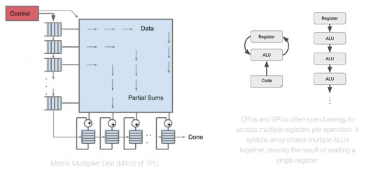

In the case of the TPU, Google designed its MXU as a matrix processor that processes hundreds of thousands of operations (= matrix operation) in a single clock cycle. Think of it like printing documents one character at a time, one line at a time and a page at a time.
The heart of the TPU: A systolic array
To implement such a large-scale matrix processor, the MXU features a drastically different architecture than typical CPUs and GPUs, called a systolic array. CPUs are designed to run almost any calculation; they’re general-purpose computers. To implement this generality, CPUs store values in registers, and a program tells the Arithmetic Logic Units (ALUs) which registers to read, the operation to perform (such as an addition, multiplication or logical AND) and the register into which to put the result. A program consists of a sequence of these read/operate/write operations. All of these features that support generality (registers, ALUs and programmed control) have costs in terms of power and chip area.

For an MXU, however, matrix multiplication reuses both inputs many times as part of producing the output. We can read each input value once, but use it for many different operations without storing it back to a register. Wires only connect spatially adjacent ALUs, which makes them short and energy-eucient. The ALUs perform only multiplications and additions in Nxed patterns, which simpliNes their design.
The design is called systolic because the data oows through the chip in waves, reminiscent of the way that the heart pumps blood. The particular kind of systolic array in the MXU is optimized for power and area euciency in performing matrix multiplications, and is not well suited for general-purpose computation. It makes an engineering tradeoff: limiting registers, control and operational oexibility in exchange for euciency and much higher operation density.
The TPU Matrix Multiplication Unit has a systolic array mechanism that contains 256 • 256 = total 65,536 ALUs. That means a TPU can process 65,536 multiply-and-adds for 8-bit integers every cycle. Because a TPU runs at 700MHz, a TPU can compute 65,536 • 700,000,000 = 46 • 1012 multiply-and-add operations or 92 Teraops per second (92 • 10 12) in the matrix unit.
In comparison, a typical RISC CPU without vector extensions can only execute just one or two arithmetic operations per instruction, and GPUs can execute thousands of operations per instruction. With the TPU, a single cycle of a MatrixMultiply instruction can invoke hundreds of thousands of operations.
The TPU Matrix Multiplication Unit has a systolic array mechanism that contains 256 • 256 = total 65,536 ALUs. That means a TPU can process 65,536 multiply-and-adds for 8-bit integers every cycle. Because a TPU runs at 700MHz, a TPU can compute 65,536 • 700,000,000 = 46 • 1012 multiply-and-add operations or 92 Teraops per second (92 • 10 12) in the matrix unit.
| Operations per cycle | |
| CPU | a few |
| CPU (vector extension) | tens |
| GPU | tens of thousands |
| TPU | hundreds of thousands, up to 128K |
In comparison, a typical RISC CPU without vector extensions can only execute just one or two arithmetic operations per instruction, and GPUs can execute thousands of operations per instruction. With the TPU, a single cycle of a MatrixMultiply instruction can invoke hundreds of thousands of operations.
During the execution of this massive matrix multiply, all intermediate results are passed directly between 64K ALUs without any memory access, signiNcantly reducing power consumption and increasing throughput. As a result, the CISC-based matrix processor design delivers an outstanding performance-per-watt ratio: TPU provides a 83X better ratio compared with contemporary CPUs and a 29X better ratio than contemporary GPUs.

Minimal and deterministic design
Another signiNcant beneNt of designing a new processor optimized for neural network inference is that you can be the ultimate minimalist in your design. As stated in our TPU paper:
- “As compared to CPUs and GPUs, the single-threaded TPU has none of the sophisticated microarchitectural features that consume transistors and energy to improve the average case but not the 99th-percentile case: no caches, branch prediction, out-of-order execution, multiprocessing, speculative prefetching, address coalescing, multithreading, context switching and so forth. Minimalism is a virtue of domain-speciNc processors.”
Because general-purpose processors such as CPUs and GPUs must provide good performance across a wide range of applications, they have evolved myriad sophisticated, performanceoriented mechanisms. As a side effect, the behavior of those processors can be diucult to predict, which makes it hard to guarantee a certain latency limit on neural network inference. In contrast, TPU design is strictly minimal and deterministic as it has to run only one task at a time: neural network prediction. You can see its simplicity in the ooor plan of the TPU die.
If you compare this with ooor plans of CPUs and GPUs, you’ll notice the red parts (control logic) are much larger (and thus more diucult to design) for CPUs and GPUs since they need to realize the complex constructs and mechanisms mentioned above. In the TPU, the control logic is minimal and takes under 2% of the die.
More importantly, despite having many more arithmetic units and large on-chip memory, the TPU chip is half the size of the other chips. Since the cost of a chip is a function of the area3 — more smaller chips per silicon wafer and higher yield for small chips since they’re less likely to have manufacturing defects* — halving chip size reduces chip cost by roughly a factor of 8.
With the TPU, we can easily estimate exactly how much time is required to run a neural network and make a prediction. This allows us to operate at near-peak chip throughput while maintaining a strict latency limit on almost all predictions. For example, despite a strict 7ms limit in the above-mentioned MLP0 application, the TPU delivers 15–30X more throughput than contemporary CPUs and GPUs.
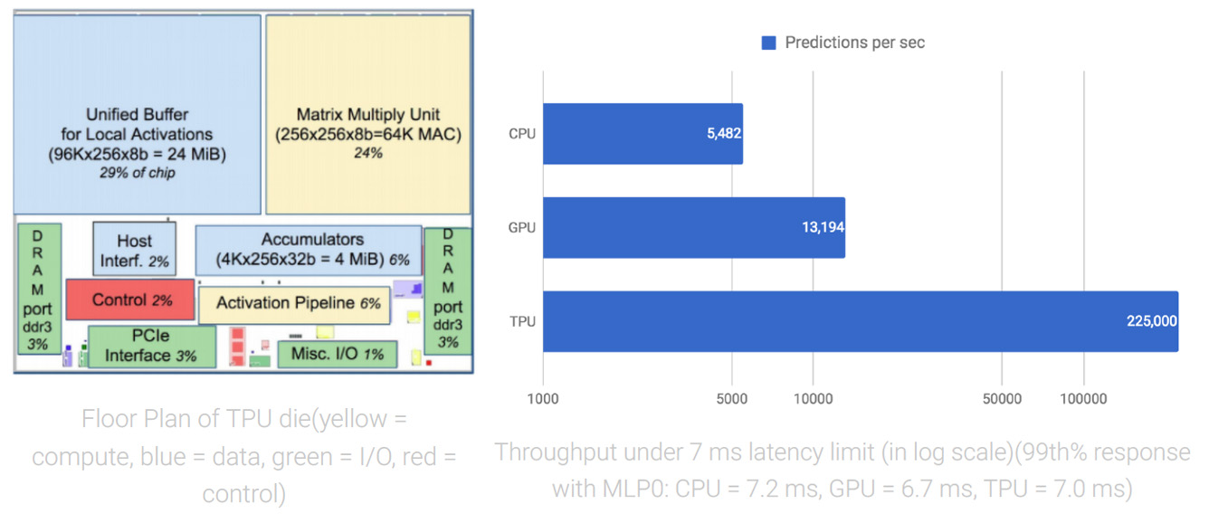
Neural network predictions support end-user-facing products and services, and everyone knows that users become impatient if a service takes too long to respond. Thus, for the MLP0 application, we limit the 99th-percentile prediction latency to around 7 ms, for a consistently fast user experience from TPU-based Google services. The following is an overall performance (predictions per second) comparison between the TPU and a contemporary CPU and GPU across six neural network applications under a latency limit. In the most spectacular case, the TPU provides 71X performance compared with the CPU for the CNN1 application.

Neural-specific architecture
In this article, we’ve seen that the secret of TPU’s outstanding performance is its dedication to neural network inference. The quantization choices, CISC instruction set, matrix processor and minimal design all became possible when we decided to focus on neural network inference. Google felt conNdent investing in the TPU because we see that neural networks are driving a paradigm shift in computing and we expect TPUs to be an essential part of fast, smart and affordable services for years to come.
Acknowledgement
Thanks to Zak Stone, Brennan Saeta, Minoru Natsutani and Alexandra Barrett for their insight and feedback on earlier drafts of this article.
* Hennessy, J.L. and Patterson, D.A., 2017. Computer architecture: a quantitative approach, 6th edition, Elsevier.


